Difference between revisions of "Ws2811 driver code explained"
From Just in Time
(Saving work in progress) |
m (Work in progress) |
||
| Line 20: | Line 20: | ||
# a graphical representation of the waveform shape that is being emitted | # a graphical representation of the waveform shape that is being emitted | ||
# jump labels, these are structurally named, more on that later | # jump labels, these are structurally named, more on that later | ||
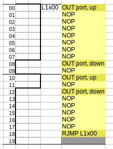
| − | # the actual instructions | + | # the actual instructions. For readability, I'm going to omit the NOP instructions in following images. |
Labels are named '''Labcd''', '''Mabcd''', '''Habcd''' or '''Pabcd'''. The digits '''cd''' encode the ''phase'' at that point (the 00 in L1x'''00'''). The digits '''ab''' represent the two-bit sequence that is being sent, with ''x'' representing "don't know" (The 1x in L'''1x'''00 means that we know that the first bit is 1 and we don't know the second bit value yet). The starting letters encode where we are in the byte: '''L''' means we may be at the last 2 bits, '''M''' means we're definately '''not''' in the last two bits, and '''H''' means that we're finishing of the last bit of the complete byte sequence. | Labels are named '''Labcd''', '''Mabcd''', '''Habcd''' or '''Pabcd'''. The digits '''cd''' encode the ''phase'' at that point (the 00 in L1x'''00'''). The digits '''ab''' represent the two-bit sequence that is being sent, with ''x'' representing "don't know" (The 1x in L'''1x'''00 means that we know that the first bit is 1 and we don't know the second bit value yet). The starting letters encode where we are in the byte: '''L''' means we may be at the last 2 bits, '''M''' means we're definately '''not''' in the last two bits, and '''H''' means that we're finishing of the last bit of the complete byte sequence. | ||
| Line 31: | Line 31: | ||
| | | | ||
===Determine second bit=== | ===Determine second bit=== | ||
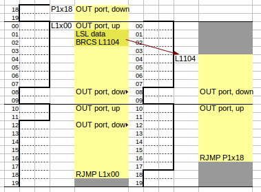
| − | Let's assume that at label ''L1x00'' we know that the first bit is a ''1'' and that | + | Let's assume that at label ''L1x00'' we already know that the first bit of the 2-bit sequence is a ''1'' and that there is a register called ''data'' that contains the second bit value in its most significant bit (and that may have even more bit values in bits 6-1). The only thing we have to do now is to shift that bit into the carry flag. If that second bit is zero, we're already at the right track, but if that bit is one, then we should switch tracks to a "11"-sequence. That switch is exactly what the highlighted code in this image does. |
| + | |||
| + | Note that the code jumps from an instruction that is in ''phase'' ''02''. Because a jump takes 2 clock ticks, it will arrive at an instruction that is in phase ''04'' (two steps further in generating the wave form). Hence the label '''L1104'''. The '''11''' means we know we're emitting the sequence 11 and the '''04''' means we're at phase 04. | ||
| + | |||
| + | Also notice that at the end of the "L1104"-block, we don't have time to jump to the "L1x00" label, because we need to push down the line (in phase ''18'') and quickly move it up again (in phase ''00''). We therefore jump sooner, in phase ''16''. But we cannot land in L1x00, because then we'd skip two clock cycles (we're jumping from phase ''16'', which means it's phase ''18'' where we land). We therefore fit two extra clock cycles to represent phases ''18'' and ''19'' before L1x00 and call these P1x18. | ||
| + | |||
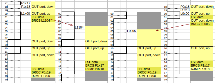
| + | Now that we've adapted the sequence to the value of the second bit of the 2-bit sequence, let's adapt to the first bit as well. Adapting to the first bit of the sequence must be done before the sequence start, therefore, at the end of the sequence we'll now add the shift-and branch instructions that will jump depending on the first bit of the next sequence. This is shown in the next picture. | ||
| + | |- | ||
| + | |colspan="2"| | ||
| + | ===Determine first bit of next sequence=== | ||
| + | [[Image:jump on first bit of next sequence.png]] | ||
| + | |||
| + | Thhe image above shows all the blocks necessary to output all four combinations of 2 bits. Every 2-bit sequence starts at either L1x00 or L0x00, depending on the value of the first bit, then depending on the value of the second bit, the code may jump to L1104 or L0005 respectively. At the end of each block the value of the first bit of the next sequence is determined and the code jumps to L1x00, L0x00 or one of its preambles (the Pnx-labels). | ||
|} | |} | ||
Revision as of 19:21, 19 May 2013
This page gives a detailed description of the WS2811@8Mhz driver code and the methodology used to create that code. The intent of the code is to send a serial signal to a given output pin in a strict 10 clockcycles/bit timing. Below follows a step-by-step explanation. You should already know a little AVR assembly language to follow the descriptions, although the code uses a very small subset of the AVR instruction set.
General description
The code contains an outer loop that loops over bytes that need to be sent. Bytes are expected in the correct order in memory, that is: in GRB order. An inner loop sends out 2 bits at a time. Essentially there are 4 variants of the inner loop, one each for the combinations 00, 01, 10 and 11.
Normally, when creating timed loops, the extra clocktick that a jump-taken uses is compensated by adding a NOP in the not-taken code path. We cannot afford such NOP instructions here, so instead each instruction is annotated with the phase within the 20-clock cycle at which it executes and care is taken that all the output signalling is done at exactly the right phase, while other instructions are performed whenever possible.


