Difference between revisions of "Ws2811 driver code explained"
From Just in Time
| (6 intermediate revisions by the same user not shown) | |||
| Line 1: | Line 1: | ||
| − | This page gives a detailed description of the WS2811@8Mhz driver code and the methodology used to create that code. The intent of the code is to send a serial signal to a given output pin in a strict 10 clockcycles/bit timing. Below follows a step-by-step explanation. | + | This page gives a detailed description of the first version of the WS2811@8Mhz driver code mentioned on the page "[[Driving the WS2811 at 800 kHz with an 8 MHz AVR]]" and the methodology used to create that code. Note that I've created a much smaller implementation since, which is described on that page. I'm leaving this text as a reference, because the method described here to create the old version of the driver is actually very similar to the one used to create the smaller one. |
| + | |||
| + | The intent of the code is to send a serial signal to a given output pin in a strict 10 clockcycles/bit timing. Below follows a step-by-step explanation. The text assumes some familiarity with AVR assembly, although the code uses a very small subset of the AVR instruction set. | ||
==General description== | ==General description== | ||
The code contains an outer loop that loops over bytes that need to be sent. Bytes are expected in the correct order in memory, that is: in GRB order. | The code contains an outer loop that loops over bytes that need to be sent. Bytes are expected in the correct order in memory, that is: in GRB order. | ||
| − | An inner loop sends out 2 bits at a time. Essentially there are 4 variants of the inner loop, one each for the combinations ''00'', ''01'', ''10'' and ''11''. | + | An inner loop sends out 2 bits at a time. Essentially there are 4 variants of the inner loop, one each for the combinations ''00'', ''01'', ''10'' and ''11''. The code will quickly determine in which of those four loops it needs to be and then perform all other tasks around the OUT-instructions that are necessary at fixed points in those four loops. |
Normally, when creating timed loops, the extra clocktick that a jump-taken uses is compensated by adding a NOP in the not-taken code path. We cannot afford such NOP instructions here, so instead each instruction is annotated with the ''phase'' within the 20-clock cycle at which it executes and care is taken that all the output signalling is done at exactly the right ''phase'', while other instructions are performed whenever possible. | Normally, when creating timed loops, the extra clocktick that a jump-taken uses is compensated by adding a NOP in the not-taken code path. We cannot afford such NOP instructions here, so instead each instruction is annotated with the ''phase'' within the 20-clock cycle at which it executes and care is taken that all the output signalling is done at exactly the right ''phase'', while other instructions are performed whenever possible. | ||
| Line 13: | Line 15: | ||
| | | | ||
===Skeleton=== | ===Skeleton=== | ||
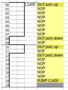
| − | This image shows code that will continuously (and endlessly) send the bit-sequence "''10''" in a strict 20-clockcycle loop. This will be the skeleton that is used to add the rest of the code. Note that the '''OUT''' instructions can't be moved to any other point in time, so these form the pillars around which the rest of the code will be added. | + | This image shows code that will continuously (and endlessly) send the bit-sequence "''10''" in a strict 20-clockcycle loop. This will be the skeleton that is used to add the rest of the code. The code starts out as 4 of those skeletons (one for "''00''", "''01''", "''10''" and "''11''") fitted with jumps from one to the other to create the right bit sequence. |
| + | |||
| + | Note that the '''OUT''' instructions can't be moved to any other point in time, so these form the pillars around which the rest of the code will be added. | ||
The code is presented in 4 columns: | The code is presented in 4 columns: | ||
| Line 30: | Line 34: | ||
|[[Image:jump on second bit value.png]] | |[[Image:jump on second bit value.png]] | ||
| | | | ||
| + | |||
===Determine second bit=== | ===Determine second bit=== | ||
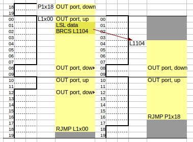
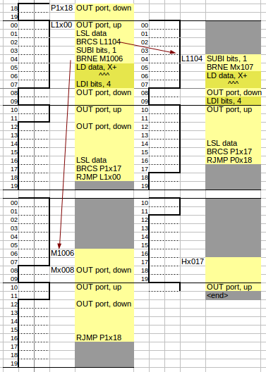
Let's assume that at label ''L1x00'' we already know that the first bit of the 2-bit sequence is a ''1'' and that there is a register called ''data'' that contains the second bit value in its most significant bit (and that may have even more bit values in bits 6-1). The only thing we have to do now is to shift that bit into the carry flag. If that second bit is zero, we're already at the right track, but if that bit is one, then we should switch tracks to a "11"-sequence. That switch is exactly what the highlighted code in this image does. | Let's assume that at label ''L1x00'' we already know that the first bit of the 2-bit sequence is a ''1'' and that there is a register called ''data'' that contains the second bit value in its most significant bit (and that may have even more bit values in bits 6-1). The only thing we have to do now is to shift that bit into the carry flag. If that second bit is zero, we're already at the right track, but if that bit is one, then we should switch tracks to a "11"-sequence. That switch is exactly what the highlighted code in this image does. | ||
| Line 64: | Line 69: | ||
| | | | ||
===Fetch the next byte=== | ===Fetch the next byte=== | ||
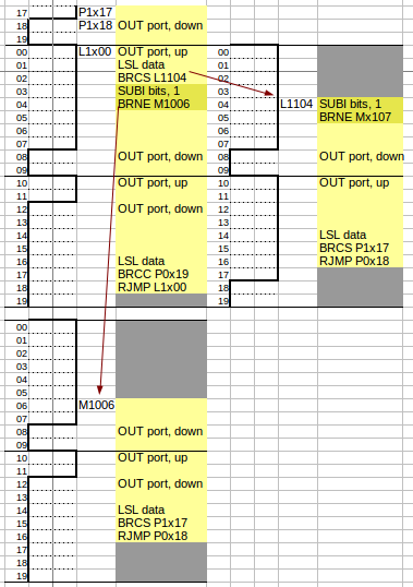
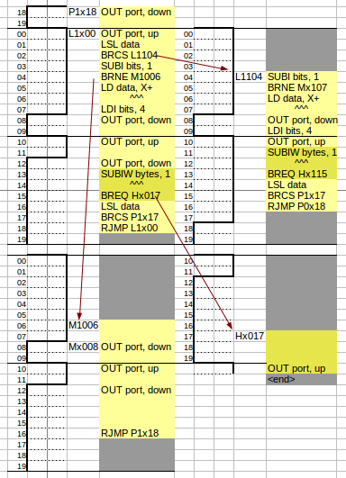
| − | Now we're ready to load the next byte and to reset the bit counter to 4. Notice here that the single instruction ''LD data, X+'' takes two clock cycles, we mark that with the "^^^" in the next clock cycle. Notice also that we have to hurry, because particularly in the L1104 block we're quickly approaching the end of the cycle. Luckily there's only one thing left to do: see if the byte | + | Now we're ready to load the next byte and to reset the bit counter to 4. Notice here that the single instruction ''LD data, X+'' takes two clock cycles, we mark that with the "^^^" in the next clock cycle. Notice also that we have to hurry, because particularly in the L1104 block we're quickly approaching the end of the cycle. Luckily there's only one thing left to do: see if the current byte is actually the last byte of the sequence. |
|- | |- | ||
|[[Image:final byte of the sequence.png]] | |[[Image:final byte of the sequence.png]] | ||
| | | | ||
| + | |||
===The final bit=== | ===The final bit=== | ||
| − | Now it's time to see if we're done completely. The code decreases a 16-bit byte counter–again a 2 cycle instruction–and jumps out if it is zero | + | Now it's time to see if we're done completely. The code decreases a 16-bit byte counter–again a 2 cycle instruction–and jumps out (to Hx017) if it is zero. |
|} | |} | ||
| Line 77: | Line 83: | ||
[[Image:ws2811 instruction table.png]] | [[Image:ws2811 instruction table.png]] | ||
| + | |||
| + | ==Comments? Questions?== | ||
| + | {{ShowComments|show=True}} | ||
| + | |||
| + | [[Category:AVR]] | ||
Latest revision as of 22:30, 11 March 2014
This page gives a detailed description of the first version of the WS2811@8Mhz driver code mentioned on the page "Driving the WS2811 at 800 kHz with an 8 MHz AVR" and the methodology used to create that code. Note that I've created a much smaller implementation since, which is described on that page. I'm leaving this text as a reference, because the method described here to create the old version of the driver is actually very similar to the one used to create the smaller one.
The intent of the code is to send a serial signal to a given output pin in a strict 10 clockcycles/bit timing. Below follows a step-by-step explanation. The text assumes some familiarity with AVR assembly, although the code uses a very small subset of the AVR instruction set.
General description
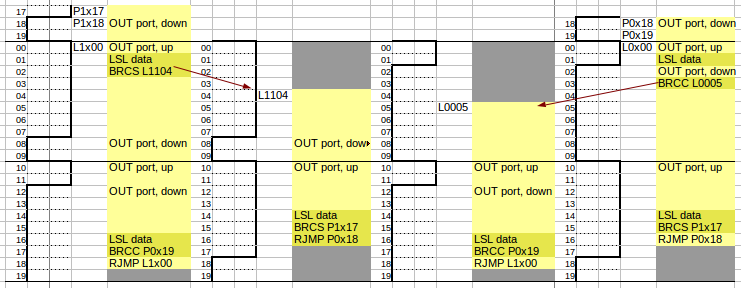
The code contains an outer loop that loops over bytes that need to be sent. Bytes are expected in the correct order in memory, that is: in GRB order. An inner loop sends out 2 bits at a time. Essentially there are 4 variants of the inner loop, one each for the combinations 00, 01, 10 and 11. The code will quickly determine in which of those four loops it needs to be and then perform all other tasks around the OUT-instructions that are necessary at fixed points in those four loops.
Normally, when creating timed loops, the extra clocktick that a jump-taken uses is compensated by adding a NOP in the not-taken code path. We cannot afford such NOP instructions here, so instead each instruction is annotated with the phase within the 20-clock cycle at which it executes and care is taken that all the output signalling is done at exactly the right phase, while other instructions are performed whenever possible.
Steps
Complete code
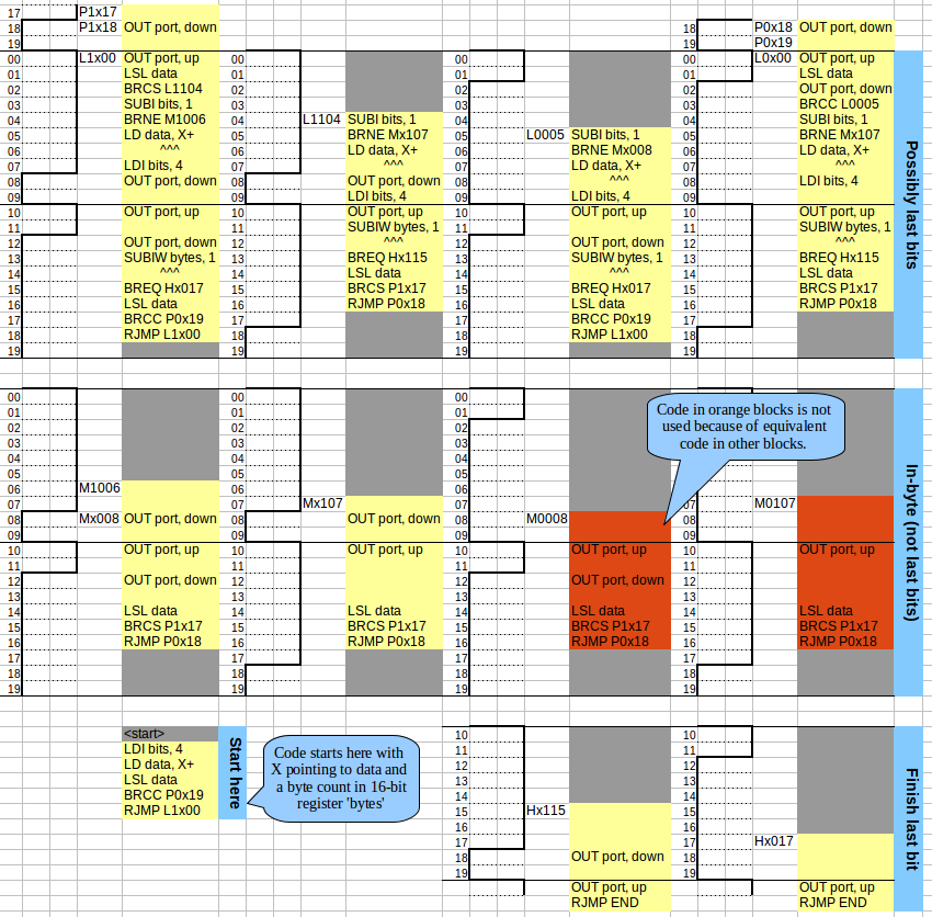
Below is the complete assembly code arranged in blocks. The orange-colored blocks M0008 and M0107 are left out of the actual code, because they are functionally equivalent to blocks starting at Mx008 and Mx107 respectively. This code is available as a spreadsheet on github. The final assembly code is also available on github. The order of the blocks in that final assembly source has been determined by a dedicated C++ program, so that all of the conditional jumps were in the allowed range.
Comments? Questions?
{{#set: |Article has average rating={{#averagerating:}} }} {{#showcommentform:}}
{{#ask: Belongs to article::Ws2811 driver code explainedModification date::+
 | ?Has comment person
 | ?Has comment date
 | ?Has comment text
 | ?Has comment rating
 | ?Belongs to comment
 | ?Comment was deleted#true,false
 | ?Has comment editor
 | ?Modification date
 | ?Has attached article
 | format=template
 | template=CommentResult
 | sort=Has comment date
 | order=asc
 | link=none
 | limit=100
}}
